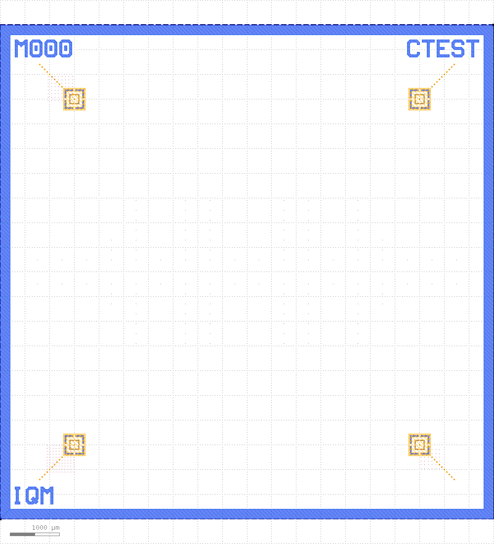
kqcircuits.chips.tsv_test
- class kqcircuits.chips.tsv_test.TsvTest[source]
Bases:
ChipThrough silicon via test chip.
Consists of arrays of TSVs and metrology segment for crossectional analysis.
array_layout (List) - Array layout for TSV in center, default=
[2, 2, 2, 6, 14, 2, 14, 14, 2, 2, 14, 14, 2, 14, 6, 2, 2, 2]metrology_pitch (Double) - Pitch in the metrology, default=
50, unit=μmcpw_distance (Double) - CPW Placeholder distance, default=
100, unit=μmhor_distance (Double) - Horizontal pitch on TSV, default=
200, unit=μmver_distance (Double) - Vertical pitch on TSV, default=
500, unit=μma (Double) - Width of center conductor, default=
10, unit=μmb (Double) - Width of gap, default=
6, unit=μmn (Int) - Number of points on turns, default=
64r (Double) - Turn radius, default=
100, unit=μmmargin (Double) - Margin of the protection layer, default=
5, unit=μmface_ids (List) - Chip face IDs list, default=
['1t1', '2b1', '1b1', '2t1']display_name (String) - Name displayed in GUI (empty for default), default=
protect_opposite_face (Boolean) - This applies only on signal carrying elements that typically include some metal between gaps., default=
Falseopposing_face_id_groups (List) - Opposing face ID groups (list of lists), default=
[['1t1', '2b1']]duplicate_face_ids (List) - Duplicate face IDs (list of lists), where the first face of each group is copied into other faces, default=
[]duplicate_layers (List) - Layers (list), which are copied into other faces when duplicate_face_ids are given, default=
['base_metal_gap', 'base_metal_gap_wo_grid', 'base_metal_addition']etch_opposite_face (Boolean) - Etch avoidance shaped gap on the opposite face too, default=
Falseetch_opposite_face_margin (Double) - Margin of the opposite face etch shape, default=
5, unit=μm_epr_show (Boolean) - Show geometry related to EPR simulation, if available, default=
False_epr_cross_section_cut (Boolean) - Show EPR cross section cuts, if available, default=
False_epr_counter (Int) - Internal counter to enable EPR preview, default=
0tsv_type (String) - TSV type, default=
Tsv Standard, choices=['Tsv Standard', 'Tsv Ellipse']tsv_diameter (Double) - TSV diameter, default=
10, unit=μmtsv_margin (Double) - TSV margin, default=
30, unit=μmtsv_elliptical_width (Double) - TSV elliptical width, default=
10, unit=μm