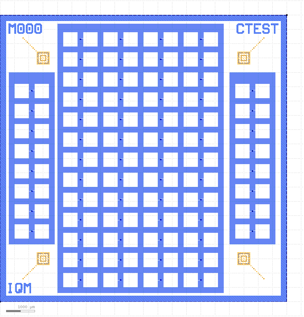
kqcircuits.chips.junction_test2
- class kqcircuits.chips.junction_test2.JunctionTest2[source]
Bases:
ChipThe PCell declaration for a JunctionTest2 chip.
pad_width (Double) - Pad width, default=
500, unit=μmjunctions_horizontal (Boolean) - Horizontal (True) or vertical (False) junctions, default=
Truesmall_loop_area (Double) - Test SQUIDs small loop area, default=
80, unit=μmlarge_loop_area (Double) - Test SQUIDs large loop area, default=
130, unit=μmjunction_width_small (Double) - Test SQUIDs Junction finger width starting value (small loop), default=
0.15, unit=μmjunction_width_large (Double) - Test SQUIDs Junction finger width starting value (large loop), default=
0.08, unit=μmjunction_width_step_increment_small (Double) - Junction finger width step increment (small loop), default=
0.01, unit=μmjunction_width_step_increment_large (Double) - Junction finger width step increment (large loop), default=
0.03, unit=μmpads_loop (List) - Select large or small loop area for each central test pad, default=
['large', 'large', 'small', 'small', 'small', 'large']marker_types (List) - Marker type for each chip corner, clockwise starting from lower left, default=
['Marker Standard', 'Marker Standard', 'Marker Standard', 'Marker Standard']junction_type (String) - Junction Type, default=
Manhattan, choices=['No Squid', 'Manhattan', 'Manhattan Single Junction', 'Super Inductor', 'Sim']a (Double) - Width of center conductor, default=
10, unit=μmb (Double) - Width of gap, default=
6, unit=μmn (Int) - Number of points on turns, default=
64r (Double) - Turn radius, default=
100, unit=μmmargin (Double) - Margin of the protection layer, default=
5, unit=μmface_ids (List) - Chip face IDs list, default=
['1t1', '2b1', '1b1', '2t1']display_name (String) - Name displayed in GUI (empty for default), default=
protect_opposite_face (Boolean) - This applies only on signal carrying elements that typically include some metal between gaps., default=
Falseopposing_face_id_groups (List) - Opposing face ID groups (list of lists), default=
[['1t1', '2b1']]etch_opposite_face (Boolean) - Etch avoidance shaped gap on the opposite face too, default=
Falseetch_opposite_face_margin (Double) - Margin of the opposite face etch shape, default=
5, unit=μm_epr_show (Boolean) - Show geometry related to EPR simulation, if available, default=
False_epr_cross_section_cut_layer (Layer) - Layer where EPR cross section cuts are placed, default=
None_epr_cross_section_cut_width (Double) - Width of the EPR cross section cuts when visualised, default=
0.0area_height (Double) - Area height, default=
1900, unit=μmarea_width (Double) - Area width, default=
1300, unit=μmpad_spacing (Double) - Spacing between different pad pairs, default=
200, unit=μmonly_pads (Boolean) - Only produce pads, no junctions, default=
Falsepad_configuration (String) - Pad configuration, default=
2-port, choices=['2-port', '4-port']junction_width_steps (List) - Automatically generate junction widths [start, step], default=
[0, 0], unit=μm, μmjunction_widths (List) - Override the junction widths with these values., default=
[]junction_test_pads_type (String) - Type of junction test pads, default=
Junction Test Pads Simple, choices=['Junction Test Pads Simple']mirror_squid (Boolean) - Mirror SQUID by its Y axis, default=
Falsefinger_overshoot (Double) - Length of fingers after the junction., default=
1.0, unit=μminclude_base_metal_gap (Boolean) - Include base metal gap layer, default=
Trueshadow_margin (Double) - Shadow layer margin near the the pads, default=
1.0, unit=μmcompact_geometry (Boolean) - Compact geometry for metal addition., default=
Falseseparate_junctions (Boolean) - Junctions to separate layer, default=
Trueoffset_compensation (Double) - Junction lead offset from junction width, default=
0, unit=μmmirror_offset (Boolean) - Move the junction lead offset to the other lead, default=
Falsefinger_overlap (Double) - Length of fingers inside the pads, default=
0.2, unit=μmsingle_junction (Boolean) - Disable the second junction, default=
False
