kqcircuits.chips.chip
- class kqcircuits.chips.chip.Chip[source]
Bases:
ElementBase PCell declaration for chips.
Produces labels in pixel corners, dicing edge, markers and optionally grid for all chip faces. Contains methods for producing launchers in face 0 and connectors between faces 0 and 1.
- LIBRARY_NAME = 'Chip Library'
- LIBRARY_DESCRIPTION = 'Superconducting quantum circuit library for chips.'
- LIBRARY_PATH = 'chips'
- static get_launcher_assignments(chip_cell)[source]
Returns a dictionary of launcher assignments (port_id: launcher_id) for the chip.
- Parameters:
chip_cell – Cell object of the chip
- produce_junction_tests(junction_type='Manhattan')[source]
Produces junction test pads in the chip.
- Parameters:
junction_type – A string defining the type of junction used in the test pads.
- produce_ground_grid()[source]
Produces ground grid on all faces with ChipFrames.
This method is called in build(). Override this method to produce a different set of chip frames.
- produce_ground_on_face_grid(box, face_id)[source]
Produces ground grid in the given face of the chip.
- Parameters:
box – pya.DBox within which the grid is created
face_id (int) – ID of the face where the grid is created
- produce_frame(frame_parameters, trans=r0 0, 0)[source]
Produces a chip frame and markers for the given face.
- Parameters:
frame_parameters – PCell parameters for the chip frame
trans – DTrans for the chip frame, default=pya.DTrans()
- merge_layout_layers_on_face(face, tolerance=0.004)[source]
Creates “base_metal_gap” layer on given face.
The layer shape is combination of three layers using subtract (-) and insert (+) operations:
“base_metal_gap” = “base_metal_gap_wo_grid” - “base_metal_addition” + “ground_grid”
- Parameters:
face – face dictionary containing layer names as keys and layer info objects as values
tolerance – gap length to be ignored while merging (µm)
- merge_layout_layers()[source]
Creates “base_metal_gap” layers on all faces.
The layer shape is combination of three layers using subtract (-) and insert (+) operations:
“base_metal_gap” = “base_metal_gap_wo_grid” - “base_metal_addition” + “ground_grid”
This method is called in build(). Override this method to produce a different set of chip frames.
- produce_structures()[source]
Produces chip frame and possibly other structures before the ground grid.
This method is called in post_build(). Override this method to produce a different set of chip frames.
- get_box(face=0)[source]
Get the chip frame box for the specified face, correctly resolving defaults.
- Parameters:
face – Integer specifying face, default 0
Returns: pya.DBox box for the specified face
- get_filter_regions(filter_layer_list)[source]
Transforms the filter_layer_list into filter_regions dictionary.
- Parameters:
filter_layer_list – tuple (layer_name, face, distance) specifying the distances to filtering layers
- Returns:
dict with distances as keys and filtering regions as values
- insert_filtered_elements(element_cell, shape_layers, filter_regions, locations, rotation=0)[source]
Inserts elements into given locations filtered by filter_regions.
- Parameters:
element_cell – pya.Cell specifying the element to be repeated in the grid
shape_layers – tuple (layer_name, face) specifying the shape layers on the element_cell
filter_regions – dict with distances as keys and filtering regions as values
locations – list of grid element locations as DPoints
rotation – element rotation in degrees
- Returns:
list of filtered grid element locations
- get_ground_bump_locations(bump_box)[source]
Define the locations for a grid. This method returns the full grid.
- Parameters:
bump_box – DBox specifying the region that should be filled with ground bumps
Returns: list of DPoint coordinates where a ground bump can be placed
- produce_launchers(sampleholder_type, launcher_assignments=None, enabled=None, face_id=0)[source]
Produces launchers for typical sample holders and sets chip size (
self.box) accordingly.This is a wrapper around
produce_n_launchers()to generate typical launcher configurations.- Parameters:
sampleholder_type – name of the sample holder type
launcher_assignments – dictionary of (port_id: name) that assigns a name to some of the launchers
enabled – list of enabled launchers, empty means all
face_id – index of face_ids in which to insert the launchers
- Returns:
launchers as a dictionary
{name: (point, heading, distance from chip edge)}
- produce_n_launchers(n, launcher_type, launcher_width, launcher_gap, launcher_indent, pad_pitch, launcher_assignments=None, port_id_remap=None, launcher_frame_gap=None, enabled=None, chip_box=None, face_id=0)[source]
Produces n launchers at default locations and optionally changes the chip size.
Launcher pads are equally distributed around the chip. This may be overridden by specifying the number of pads desired per chip side if
nis an array of 4 numbers.Pads not in
launcher_assignmentsare disabled by default. Theenabledargument may override this. If neither argument is defined then all pads are enabled with default names.- Parameters:
n – number of launcher pads or an array of pad numbers per side
launcher_type – type of the launchers, “RF” or “DC”
launcher_width – width of the launchers
launcher_gap – pad to ground gap of the launchers
launcher_indent – distance between the chip edge and pad port
pad_pitch – distance between pad centers
launcher_frame_gap – gap of the launcher pad at the frame
launcher_assignments – dictionary of (port_id: name) that assigns a name to some of the launchers
port_id_remap – by default, left-most top edge launcher has port_id set to 1 and port_ids increment for other launchers in clockwise order. port_id_remap is a dictionary [1..n] -> [1..n] such that for port_id_remap[x] = y, x is the port_id of the launcher in default order and y is the port_id of that launcher in your desired order. For example, to flip the launcher order by chip’s y-axis, set port_id_remap to
{i+1: ((n - i + n/4-1) % n) + 1 for i in range(n)}enabled – optional list of enabled launchers
chip_box – optionally changes the chip size (
self.box)face_id – index of face_ids in which to insert the launchers
- Returns:
launchers as a dictionary
{name: (point, heading, distance from chip edge)}
- make_grid_locations(box, delta_x=100, delta_y=100, x0=0, y0=0)[source]
Define the locations for a grid. This method returns the full grid.
- Parameters:
box – DBox specifying a region for a grid
delta_x – Int or float specifying the grid separation along the x dimension
delta_y – Int or float specifying the grid separation along the y dimension
x0 – Int or float specifying the center point displacement along the x-axis
y0 – Int or float specifying the center point displacement along the y-axis
Returns: list of DPoint coordinates for the grid.
- get_ground_tsv_locations(tsv_box, **kwargs)[source]
Define the locations for a grid. This method returns the full grid.
- Parameters:
box – DBox specifying the region that should be filled with TSVs
kwargs – additional keyword arguments
Returns: list of DPoint coordinates where a ground bump can be placed
with_grid (Boolean) - Make ground plane grid, default=
Falsegnd_grid_faces (List) - Faces on which the grid is generated, [-1] is all, [] is None, default=
[-1]merge_base_metal_gap (Boolean) - Merge grid and other gaps into base_metal_gap layer, default=
Falsea_capped (Double) - Width of center conductor in the capped region (μm), default=
10, unit=μmb_capped (Double) - Width of gap in the capped region , default=
10, unit=μmwith_gnd_tsvs (Boolean) - Make a grid of through-silicon vias (TSVs), default=
Falsetsv_grid_spacing (Double) - TSV grid spacing (center to center), default=
300, unit=μmedge_from_tsv (Double) - TSV grid clearance to chip edge (center to edge), default=
550, unit=μmtsv_edge_to_tsv_edge_separation (Double) - TSV grid clearance to existing TSVs (edge to edge), default=
250, unit=μmtsv_edge_to_nearest_element (Double) - TSV grid clearance to other elements (edge to edge), default=
100, unit=μmwith_gnd_bumps (Boolean) - Make a grid of indium bumps, default=
Falsebump_grid_spacing (Double) - Bump grid spacing (center to center), default=
120, unit=μmedge_from_bump (Double) - Bump grid clearance to chip edge (center to edge), default=
550, unit=μmbump_edge_to_bump_edge_separation (Double) - Bump grid clearance to existing bumps (edge to edge), default=
95, unit=μmbump_edge_to_metal_gap (Double) - Bump edge clearance to metal gap, default=
20, unit=μmframes_enabled (List) - List of face ids (integers) for which a ChipFrame is drawn, default=
[0]frames_marker_dist (List) - Marker distance from edge for each chip frame, default=
[1500, 1000], unit=[μm]frames_diagonal_squares (List) - Number of diagonal marker squares for each chip frame, default=
[10, 2]frames_mirrored (List) - List of booleans specifying if the frame is mirrored for each chip frame, default=
[False, True]frames_dice_width (List) - Dicing street width for each chip frame, default=
[200, 140], unit=[μm]frames_dice_grid_margin (List) - Dicing street margin for each chip frame, default=
[100, 100], unit=[μm]face_boxes (Shape) - List of chip frame sizes (type DBox) for each face. None uses the chips box parameter., default=
[None, (1500,1500;8500,8500)]dice_grid_margin (Double) - Margin of the ground grid avoidance layer for dicing edge, default=
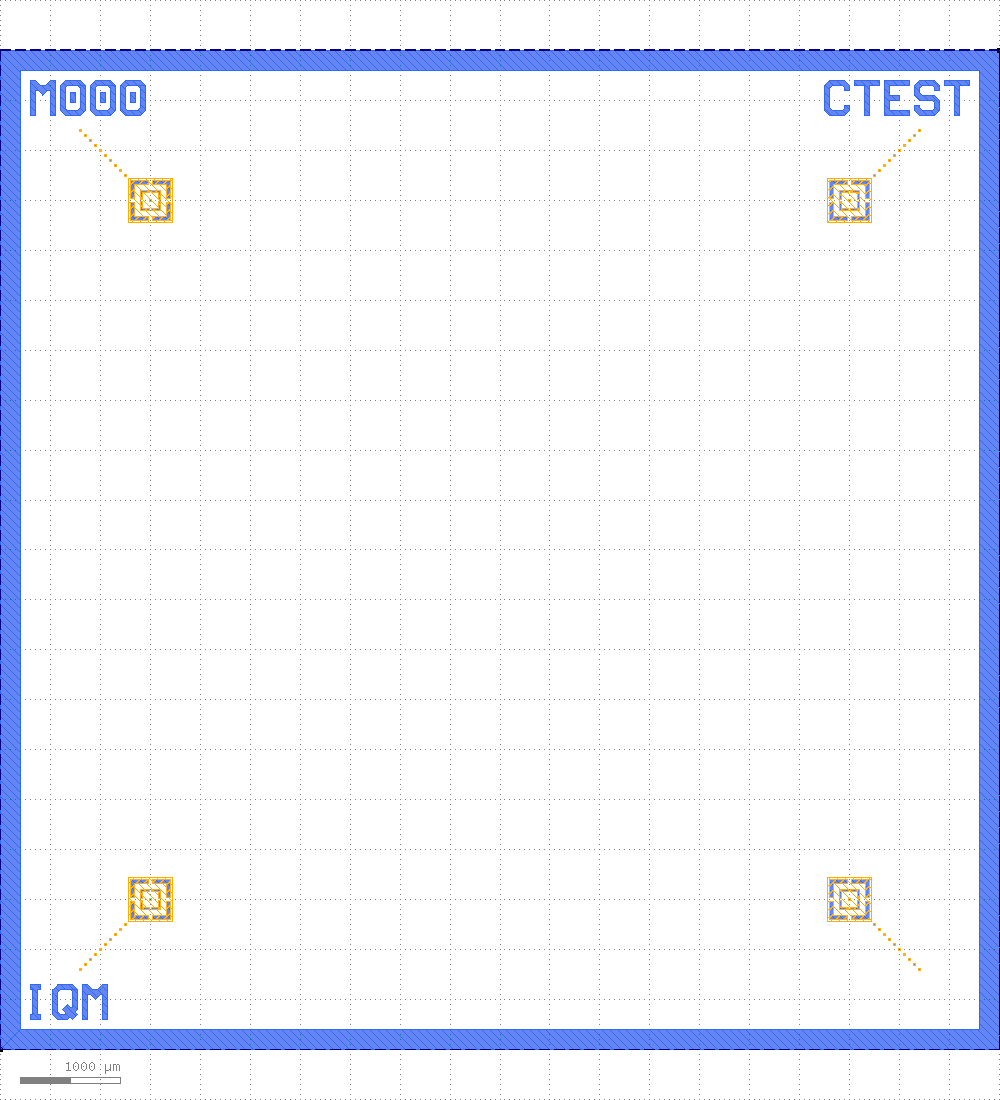
100name_mask (String) - Name of the mask, default=
M000name_chip (String) - Name of the chip, default=
CTestname_copy (String) - Name of the copy, default=
Nonename_brand (String) - Name of the brand, default=
IQMmarker_types (List) - Marker type for each chip corner, clockwise starting from lower left, default=
['Marker Standard', 'Marker Standard', 'Marker Standard', 'Marker Standard', 'Marker Standard', 'Marker Standard', 'Marker Standard', 'Marker Standard']chip_dicing_in_base_metal (Boolean) - Insert chip dicing lines in base metal addition, default=
Falsebox (Shape) - Bounding box of the chip frame, default=
(0,0;10000,10000)bump_type (String) - Bump type, default=
Flip Chip Connector Dc, choices=['Flip Chip Connector Dc']tsv_type (String) - TSV type, default=
Tsv Standard, choices=['Tsv Standard', 'Tsv Ellipse']